


Een gids voor het overstappen van prototypes van breadboard-PCB's naar volledig product
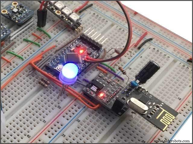
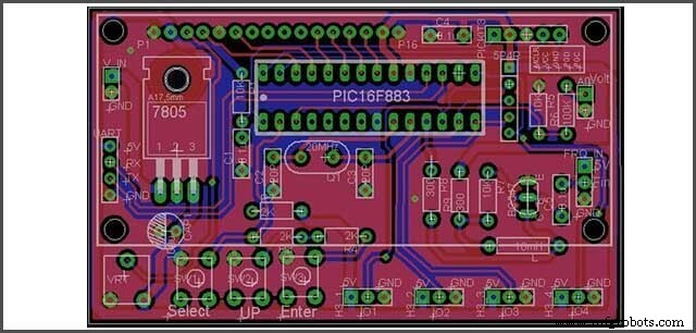
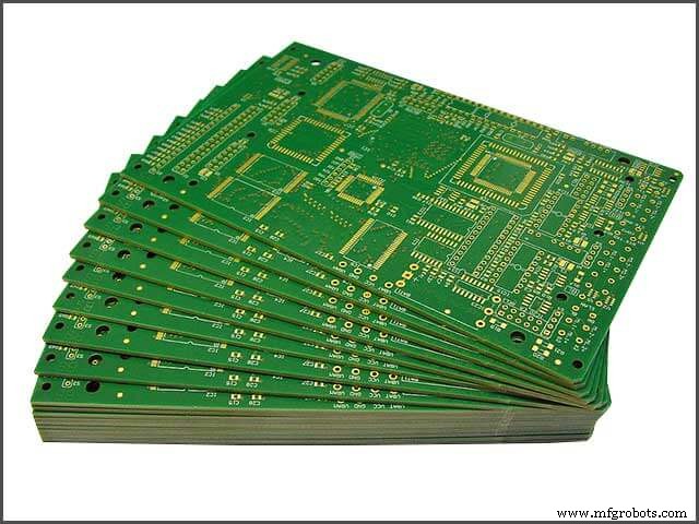
Schalen vanaf prototypes van breadboard-PCB's is een ingewikkeld proces dat creativiteit en procedures combineert. De tijdlijn voor ontwikkeling is net zo individueel als de persoon die het project uitvoert, en alles is altijd in handen van de maker. Er zijn echter verschillende mijlpalen om onderweg naar te zoeken. Breadboard-printplaat
https://youtu.be/HAOvEPh8hms
Aan de slag met het bouwen van uw PCB-prototypes
Dus nu heb je dit fantastische idee of, beter nog, een PoC (Proof of Concept), maar je moet opschalen naar iets dat massaproductie waard is of op zijn minst door sommige fabrikanten kan worden gefabriceerd voor demo-doeleinden; hoe ga je aan de slag met het bouwen van je PCB-prototypes?
Bij hardware-ontwerp zijn PCB-prototypes een "handgemaakt" model dat een gefabriceerd (gemakkelijk repliceerbaar) product vertegenwoordigt dat voldoende is voor ontwerpers om het ontwerp te visualiseren en te testen. Het woord prototype komt van de Latijnse woorden proto, wat origineel betekent, en typen, wat vorm of model betekent.
Met alle tutorials die er zijn en het aantal gratis bronnen dat beschikbaar is, wordt het voor bijna iedereen mogelijk om binnen een paar uur snelle PCB-prototypes te bouwen. Uw PCB-prototypes naar een plaats brengen waar ze kunnen worden gecommercialiseerd, kost veel inspanning, planning en enige expertise. U moet een groot aantal beslissingen nemen over hardware, die uiteindelijk leiden tot beslissingen over de apparaatsoftware. Breadboard-printplaat
Het is gemakkelijk te bouwen met een Raspberry Pi of zelfs de populaire Arduino, maar de kans dat je daarmee massaal kunt produceren is meestal beperkt. Dit betekent natuurlijk niet dat je onmogelijk een bord op het Arduino-bord kunt bouwen zoals de Arduino Pro Mini of die Arduino zonder hoofd kan aansluiten en dan zoiets gaan fabriceren. Toch kunnen ze behoorlijk duur worden en zelfs krachtiger zijn dan je nodig hebt.
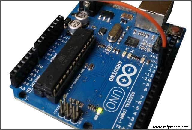
Veel van de hedendaagse hardware-startups hebben hun eerste PCB-prototypes gebouwd met Arduino . Arduino is gemakkelijk te leren, zelfs zonder een elektrotechnische achtergrond of alleen de nodige programmeervaardigheden. Zelfs een kind zou het kunnen, en veel van hen doen het.
1.1 Breadboard-printplaat —Componentenselectie
De eerste stap om aan de slag te gaan met het bouwen van uw PCB-prototypes, is weten welke componenten u nodig heeft. U kunt er snel een idee van krijgen op basis van uw blokschema of bestaande PoC, en zelfs de gewenste functies van het apparaat kunnen dat snel vertellen. Bijvoorbeeld iets bouwen als een draagbare hartslagmeter vereist een aantal van de volgende zaken:
1. Een Microcontroller-eenheid - Atmega, ARM, PIC en andere
2. Een pulssensor – Een speciale pulssensor zou kunnen werken, of een combinatie van LED en lichtdetector zou ook kunnen werken.
3. Voedingseenheid
4. Een weergave-interface - LCD, LED, OLED, TFT of andere.
Men kan gemakkelijk de meeste en zo niet alle benodigde onderdelen uitbesteden van een enkele elektronicaleverancier en in sommige gevallen van meerdere leveranciers. Hier volgen enkele leveranciers waar u uw gegevens kunt kopen - AliExpress, Digi Key, Arrow, Mouser, Adafruit en verschillende andere.
1.2 Schematisch ontwerp
De volgende stap is het maken van een diagram van het elektronica-ontwerp, meestal een schematisch diagram genoemd. of een schakelschema. De schematische tekening laat zien hoe elk onderdeel aansluit, en dit is niet iets dat je met de hand doet, maar een uniek hulpmiddel dat voor dit doel is ontworpen.
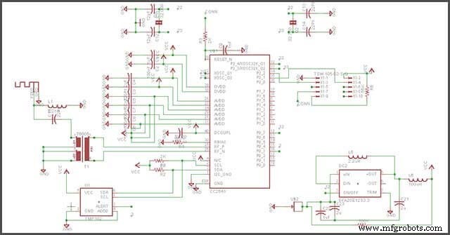
Het maken van een schema is een kernstap bij het bouwen van uw uiteindelijke apparaat en u kunt het zich niet veroorloven om het over te slaan. Aan de slag gaan met uw schema is heel eenvoudig; je moet de juiste tool kennen om te bouwen. Er kunnen verschillende circuitontwerpsoftware worden gebruikt voor schematisch ontwerp, sommige zijn gratis en sommige zijn betaalde versies. De meeste ontwerpsoftware kan worden gebruikt voor schematische tekeningen en ook voor het maken van uw PCB-lay-out.
Hieronder staan enkele software die kan worden gebruikt:
1. KiCAD – Gratis te gebruiken.
2. Eagle CAD – Premium maar met de beperkte gratis optie
3. Altium – Premium
4. DipTrace – Premium
5. OrCAD – Premium maar biedt een gratis proefperiode.
Nadat je hebt besloten welke ontwerpsoftware je wilt gebruiken, kun je jezelf vertrouwd maken met de softwareomgeving, omdat elke software er anders uitziet en aanvoelt.
Bij het maken van uw schema met uw software naar keuze, moet u een aantal standaardpraktijken volgen bij het ontwerpen van schema's.
Sommige conventionele methoden worden hieronder gemarkeerd –
1. Gebruik een knooppuntstip om meer dan één verbinding aan te geven die in een knooppunt wordt aangesloten.
2. Gebruik een netnaam voor pinnen in plaats van honderden verbindingen rond te trekken. Dit verbetert de leesbaarheid van een schema zonder onnodige rommel toe te voegen.
3. Altijd hetzelfde symbool gebruiken voor hetzelfde apparaat
4. Scheiden van uw schema in logische blokken, vooral bij het ontwerpen van een aantal complexe circuits.
Wanneer u klaar bent met uw schematisch ontwerp en het volledig hebt gecontroleerd, is de volgende stap het converteren van het circuitontwerp naar productie-PCB's; er zijn grote kansen op lay-outfouten, die een grote negatieve invloed kunnen hebben op de functionaliteit van het eindproduct. Er worden verschillende PCB-lay-outs gebruikt om uw bord te vervaardigen.
In het volgende hoofdstuk praten we over het maken van een printplaat voor je PCB-prototypes.
Een printplaat maken voor uw PCB-prototypes
Een printplaat maken voor uw PCB-prototypes, ten eerste is het hebben van een schematisch diagram een stap in het proces van een volwaardig professioneel bord.
De volgende fase van het proces, die niet kan worden overgeslagen, is het ontwerpen van de lay-out van uw printplaat. Wat is echter een printplaat?
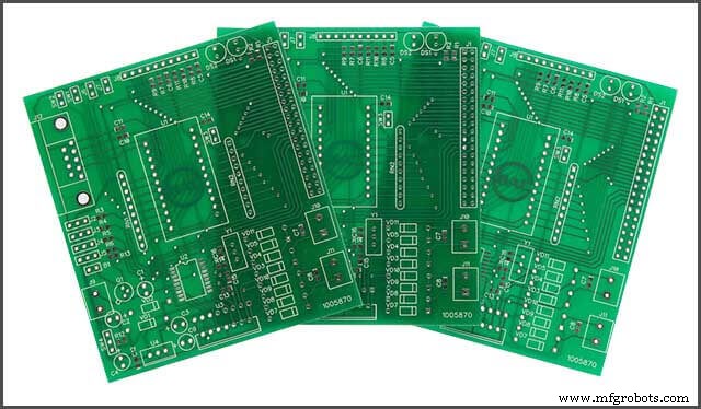

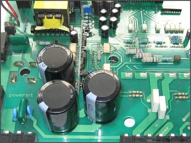
Een Printplaat , ook wel PCB genoemd, is een fysiek bord dat alle elektronische componenten op één plek vasthoudt en verbindt. Het schematische ontwerp wordt meestal op verschillende manieren op de printplaat overgebracht. Het ontwerp van de printplaat beïnvloedt een aantal factoren zoals
1. Kosten - Hoe belangrijker het bord, hoe duurder het is om te maken.
2. Prestaties - Het ontwerp van de kaart en het type gebruikte componenten zijn van invloed op de algehele prestaties van het apparaat. Een slecht ontworpen bord kan gevoelig zijn voor ruis, wat op zijn beurt de prestaties van het apparaat verslechtert.
3. Duurzaamheid,
4. En nog veel meer.
Zodra het schema klaar is, gaan we aan de slag om de PCB te maken.
De PCB is ontworpen in dezelfde software die werd gebruikt bij het maken van het schematische diagram.
De software is verantwoordelijk voor het genereren van de PCB-lay-out en footprint op basis van de gegeven componenten en het schematische diagram; zonder het schematische diagram zal de software de basisprintplaatlay-out niet maken.
Aan de slag gaan met het maken van een PCB-layout kan tijdrovend en vervelend zijn voor nieuwe gebruikers. Toch zijn er gelukkig verschillende handige tutorials en bronnen online voor de meeste PCB-software om te leren hoe ze te bouwen.
Afhankelijk van de gekozen software, is er meestal een manier waarop de gebruiker kan overschakelen van de schematische weergave naar de PCB-layoutweergave waar de PCB zal worden ontworpen.
Ontwerp uw PCB zoals u zich uw uiteindelijke apparaatmodel voorstelt; ook zal de gebruikte software verschillende verificatietools hebben om ervoor te zorgen dat de PCB-lay-out voldoet aan de ontwerpregels voor het gebruikte PCB-proces en dat de PCB overeenkomt met het schema. U kunt snel testen of uw ontwerp uw apparaat zal breken of niet.
Hoe kleiner het product en hoe strakker de componenten op elkaar moeten worden gepakt, hoe langer het duurt om de printlay-out te maken. Als uw product grote hoeveelheden stroom omleidt of draadloze connectiviteit biedt, is de lay-out van de printplaat nog kritischer en tijdrovender.
De essentiële onderdelen van de meeste PCB-prototypeontwerpen zijn stroomroutering, hogesnelheidssignalen (kristalklokken, enz.) En draadloze circuits.
Nadat u het ontwerp van uw PCB-prototype hebt aangevuld, moet u doorgaan met het vervaardigen van uw printplaat, en er zijn verschillende manieren om dit voor elkaar te krijgen. Maak het zelf thuis of stuur het ontwerp naar een fabrikant die gespecialiseerd is in het maken van PCB's.
Hoewel er technieken zijn om uw PCB's thuis te produceren, zijn deze beperkt tot eenvoudige ontwerpen. U zult dus hoogstwaarschijnlijk de productie van uw PCB-prototypes moeten uitbesteden.
In het volgende hoofdstuk hebben we het over het vervaardigen van uw printplaat door een externe fabrikant.
Uw printplaat vervaardigen met WellPCB
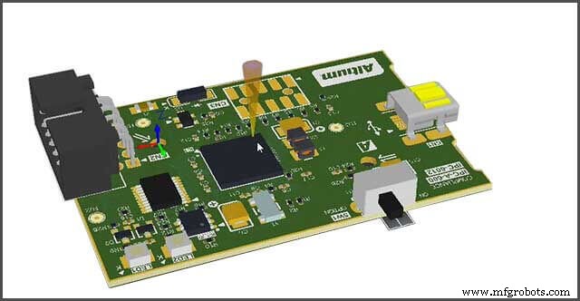
Nadat u de lay-out van de printplaat voor uw apparaat met succes hebt ontwikkeld, moet u het volgende doen om het bord te maken. Voordat u met de productie begint, is het altijd een goed idee om te zien hoe het eindproduct eruit zal zien. Sommige software zoals Proteus of Altium heeft een 3D-layoutviewer waarmee je het bord in 3D kunt bekijken om te voelen hoe het bord eruit zal zien.
Voordat u uw ontwerp opstuurt om te worden vervaardigd, moet u eerst een bestandsformaat genereren waarmee de fabrikant zal werken en beslissen wat u gaat gebruiken. WellPCB is een leider in productie.
Printplaat en de beste keuze voor uw printopdrachten.
Het PCB-ontwerp moet worden omgezet naar een Gerber-bestand dat de meeste professionals gebruiken, de standaard voor de PCB-industrie. Een Gerber-bestand bevat alle benodigde ontwerpbestanden om te gebruiken bij de productie van PCB's. WellPCB accepteert vier bestandsindelingen (Gerber-, pcb-, pcbdoc- of cam-bestandsindeling).
WellPCB bedrukt een zeefdruk aan beide zijden, en dit zonder extra kosten. Het is handig om onderdeelnummers op de bedrukte zeefdruklaag te vermelden. Het is ook een goed idee om de specificatie van het board house te kennen. WellPCB heeft een minimum van 3mil voor lijn/spoorbreedte en ruimte. Zorg ervoor dat uw ontwerp dat niet overschrijdt. Gebruik uw software-ontwerpregelcontrole om ervoor te zorgen dat uw bord de productiecapaciteiten van de fabrikant niet overschrijdt.
Zeefdrukvereisten vermelden de gewenste kleur op de printplaat, en de meeste zijn UV-uitgeharde inkten en voldoen aan RoHS.
1. Wit
2. Geel
3. Zwart
Dat zijn de meest gebruikte kleuren; andere zijn ook beschikbaar en kleuren kunnen de verwerkingstijd en -kosten verhogen.
Om uw PCB op WellPCB te bestellen, volgt u deze eenvoudige stappen:
4. Bezoek de WellPCB PCB Online Quote-sectie - https://www.wellpcb.com/pcb-quote
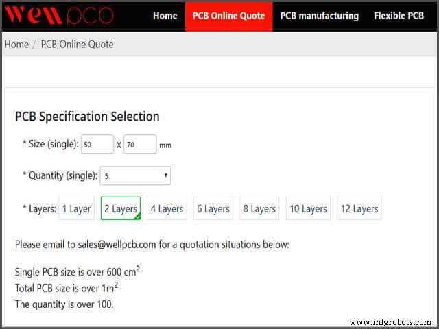
5. Vul je boardgegevens in en klik op toevoegen aan winkelwagen. Noodzaak om te weten over het online bestellen van aangepaste PCB-printplaten. VOOR de printplaat die u nodig heeft, kunt u contact met ons opnemen via WellPCB, de minimale hoeveelheid is vijf eenhedenBreadboard PCB
6. Registreer een nieuw account.
7. Upload uw PCB Gerber of. BRD-bestanden.
8. Bestel je artikel en wacht tot het wordt afgeleverd.
WellPCB helpt ook bij het uitvoeren van een volledige DRC-controle van alle bestanden van de klant, wat handig is, vooral als het ontwerp problemen of fouten bevat. De gebruiker wordt op de hoogte gesteld van het probleem om te voorkomen dat er tijd en geld wordt verspild tijdens de productie van het bord.
Nu ga je zitten en wacht je tot je printplaat arriveert. De doorlooptijd van de PCB-fabricage voor zijn PCB-services is minimaal 24 uur en een minimumtijd van ongeveer 120 uur voor een 8 - 12 laags PCB.
In het volgende hoofdstuk zullen we het hebben over enkele PCB-termen en WELLPCB-mogelijkheden.
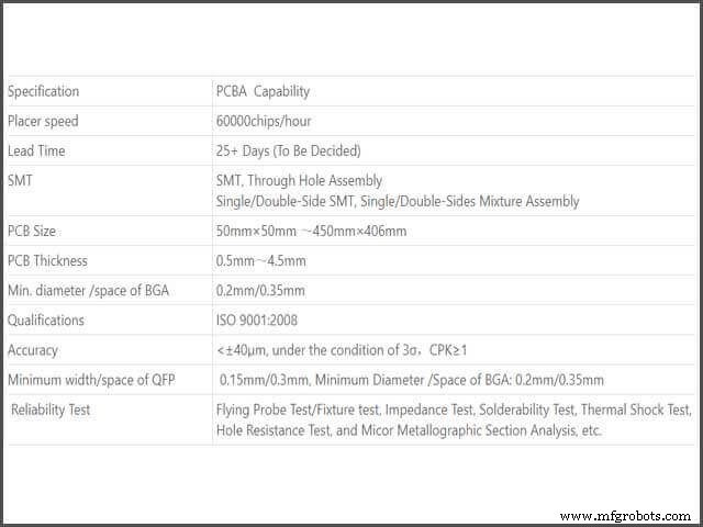
WellPCB PCB-mogelijkheden en enkele algemene PCB-termen
WellPCB is een toonaangevende fabrikant van printplaten en biedt printplaatassemblage aan bij zijn PCB-prototypes.
This makes WellPCB your go-to manufacturer for your entire product development. Also, they provide Turnkey services for outsourcing the components for your electronic board. Breadboard PCB
WellPCB is focused on offering PCB prototypes services and not just large-scale manufacturing. Their PCB prototypes services go at a minimum of 5 units. Not only are they offering prototyping services but also packaged at some meager prices.
A promotional price of $3.99 for users looking for 1-2 layers, 10pcs PCB prototypes, and a board of less than 10cm*10cm.
WELLPCB is capable of producing 100,000 square feet of 2-32-layer PCBs and delivering over 5000 varieties monthly.
With a quick turn to meet 24-hour delivery for double-sided PCBs, 48-hour for 4 to 8 layers, and 120-hour for ten layers or higher PCBs. Their standard lead time is about 5 – 6 days and an Expedited time of 24 – 48 hours.
4.1 The following are WellPCB PCB manufacturing capabilities
1. Support Material:FR4, High TG FR4, Halogen Free material, CEM-3, Rogers HF material.
2. Layer counts 1-32 layers.
3. Finished Copper Thickness:0.5-5 oz.
4. Finished Board Thickness:0.2-6.0mm.
5. Min. Line/Track Width:4mil.
6. Min. Line/Track Space:4mil.
7. Min. Contour Tolerance:+/-0.1mm.
8. Min. Finished Diameter of PTH Hole:0.1mm.
9. Max. Board Thickness/Hole Ratio:12:1.
10. Min. Solder Mask Bridge:4mil (Min. SMT Pad Space 8mil).
11. Min. Legend(Silkscreen) Track Width:5mil.
12. Solder mask color:green, black, blue, white, yellow, matt, etc.
13. Solder mask hardness:6H.
14. Legend/Silkscreen Color:white, yellow, black, etc.
15. Surface Treatment:HAL, Lead-Free HAL, Immersion gold, OSP, Immersion Tin, Immersion silver, etc.
16. Other Technology:Gold finger, peelable mask, Non-across blinded vias, characteristic impedance control, Rigid-flex board, etc.
17. Reliability Test:flying probe test/fixture test, impedance test, solderability test, thermal shock test, hole resistance test.
18. Flammability:94V-0.
4.2 Breadboard PCB —Surface Finish
A PCB surface finish is a coating between a component and a bare board PCB. It is applied for two primary reasons:to ensure solderability and to protect the exposed copper circuitry.
Standard surface finishes preference – Non-RoHS or RoHS compliant.
1. HASL (Hot Air Solder Level) – Contains Lead non-RoHS, cheaper and quite popular.
2. ENIG (Electroless Nickel Immersion Gold) – Most popular finish and lead-free, but expensive
3. Immersion Silver – RoHS compliant will tarnish like any silver product
4. OSP – Organic Solderability Preservative
5. LF-HASL (Lead-Free Hot Air Solder Level)
6. Immersion Tin – Used the least of all finishes
4.3 Soldermask
Soldermask is the color to be used for the PCB prototypes finish. Any color can be used. However, sticking to standard colors is the best and more professional. The most popular are:
1. Green
2. Blue
3. Black
4. Red
5. White
6. Yellow
Mask can be in either Matte or Gloss in those above colors. Matte is less readily available due to Gloss is most widely used. Processing Matte for specific colors may add time due to equipment change and processing cleans up and application.
4.4 Breadboard PCB —Silkscreen
Silkscreen is the printing done on the PCB for identification. It is used on the component side to identify components, test points, PCBA part numbers, warning symbols, company logos, and manufacturer names. The following are some of the colors being used:
1. Black
2. White
3. Yellow
Those are the most widely used colors; others are available; however, colors can add to process time and cost like MASK. Ask if you have special requirements for your product.
In the next chapter, we will talk about how to move your PCBA mode.
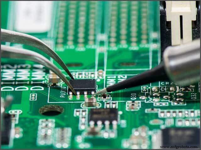
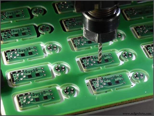
Breadboard PCB–Moving from PCB Prototypes to PCBA
So, what’s PCB Rapid Prototyping. PCB assembly. Directly speaking, PCB Rapid Prototyping. PCB assembly. Directly speaking, PCB Rapid Prototyping. 3D PCB Printing makes the PCB and does the Printed Circuit Board Assembly (PCBA, an abbreviation for printed circuit board assembly, which refers to the combination of PCB prototypes manufacture, components sourcing, and B3D PCB Printing makes the PCB and does the Printed Circuit Board Assembly PCBA is the PCB with components assembled).
So now you have your printed circuit board available and ready to populate the board with the needed components. You might be tempted to solder this manually yourself. This might be a good option, especially when the number of panels is less than five or, worst case, ten units; anything more than that might not be a good idea but going the route of PCB Rapid Prototyping. 3D PCB Printing not only makes the PCB but also does the Printed Circuit Board Assembly PCBA.
5.1 Breadboard PCB —Assembly Types of PCBA
The main assembly types of PCBA are shown below:
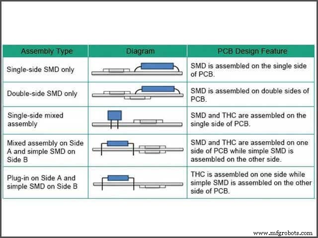
Those are the commonly used PCB Rapid Prototyping. 3D PCB Printing makes the PCB and does the Printed Circuit Board Assembly (PCBA assembly types. SMD means Surface Mount Devices, and THC implies Through Hole Components).
PCBA helps engineers, product developers, hobbyist and others to self-populate the board with needed components by a manufacturing firm.
It is usually faster and cheaper on bulk orders. Getting started with PCB Rapid Prototyping. 3D PCB Printing makes the PCB, and does the Printed Circuit Board Assembly (PCBA is also relatively simple as far you have the necessary resources).
Just like, WellPCB is capable of handling all your possible PCB prototypes works, they also offer an accompanying production film work that you require to manufacture PCBs. In the case of PCBA service to help one streamline the whole board development process. It does not cost much more to have the PCB populated unless you tack on additional steps in the process, such as burning a program to the MCU or running 100% test on the finished boards.
To get started with PCBA, you need to have all the required documents.
Aside from your PCB prototypes design file, you will need a design specification if there are special needs for your work, a bill of the material (BoM) list for the number of components on your board and also can be generated from the software being used, and part placements made from the software used.
When starting your PCB Assembly, one crucial take note is the sourcing of the components for the board.
The board owner can decide to source for the parts alone and send them to WELLPCB for assembly or let WellPCB handle the integral components sourcing, which I feel is better. Of course, partial supply can also be agreed upon.
Go to PCB Assembly on WellPCB here and fill the Request for Quotation (RFQ) form. Input as many details as possible and send it. WellPCB will get in touch if they need more information from you and continue the assembly process order.
The WellPCB Bill Of Materials (BOM) of a PCB gets fitted onto aboard. PCB Assembly process can take up to around 25 days for large volume manufacturing, which is an excellent time for large volume PCB assembly compared to other PCB Assembly manufacturers. This will make it easy for a pick and place machine to easily pick and place the components on the PCB Assembly capabilities:
More information about WellPCB SMT). This will make it easy for a pick and place machine to easily pick and place the components on the PCB Assembly capability can be found here.
At this point, all you have to do is to sit down and wait for your populated PCB to be available and sent to you. This concludes the end of this chapter, and the next chapter will discuss how to save money when doing PCB and PCBA.
Saving Money in PCB Prototypes and PCBA Manufacturing
Now congratulation, you have your fully developed hardware PCB prototypes or, better still, hardware board. For newbies, this will have been a good experience, and also a lot of money must have been sent which could have been avoided.
Some of the money spent could have been avoided due to unnecessary complexity and errors in the PCB and circuit design.
This chapter will show some of the handy tips and tricks that can help you save even millions when doing large volume manufacturing.
6.1 Breadboard PCB —Keep Your Board Size at a Minimum
Keeping your board size at a minimum is crucial in saving costs and making your final product as portable as possible. The bigger it gets, so do the prices. If the board becomes smaller, so does the cost.
Also, making your board too small might not save you cost since assembling and preparing your board might require specialized equipment.
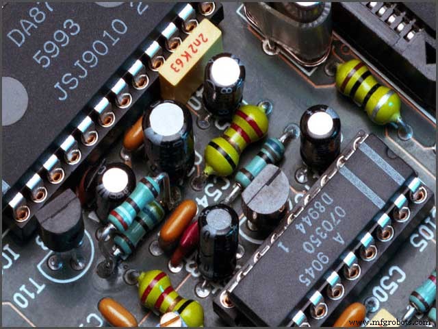
6.2 Using Surface Mount Components as Much as Possible
You might be tempted to use DIP (dual in-line) package, commonly known as Through-hole components, because it’s possible to easy to use but might not be the best cost-saving option.
1. Using surface mount components will reduce the number of holes that need to be drilled on your board typically used for through-hole parts.
2. Using surface mount components will also reduce the board size.
3. Using surface mount components will make the board assembly faster and lesser equipment used.
6.3 Set Your Design Up for Penalization
By going on board penalization, you can save yourself a ton of money. Getting all of your boards on one panel means that a rapid-fire pick and place machine can get all your parts placed in one go without requiring any additional setup time.
6.4 Silk Screening Help You Reduce Your PCB prototypes Costs?
Requesting silk screening on one side will cut your artwork costs in half. Sticking with standard colors and larger geometries will also prove beneficial. Understanding these constraints can help you to better PCB prototypes pricing and cost savings.
6.5 Breadboard PCB —Use the Right Via for the Job
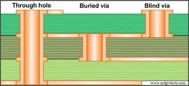
There are three types of vias – through-hole vias, blind vias, and buried vias. The last two are only going to be used for high-density and high-frequency PCBs. So, this one is simple, if your design doesn’t need these types of vias, leave them out to avoid any extra manufacturing costs.
This concludes the end of this chapter and the end of this guide. Using standard materials and several of these tips mentioned above can save you several thousand to millions of dollars when embarking on large volume manufacturing.
Breadboard PCB–Conclusion
When building and launching your products to market, some other things also need to be considered.
1. Certifications – Every wireless-based product needs to go through some certification process to be clear of any hazards or issues and be permitted to the market.
2. Enclosure – Depending on the type of product you are building, you might need some enclosure around your board to give it some artistic look or for some reason.
3. Quality Control – Quality control issues a formal inspection report for review and shipment approval. You should expect each shipment to be inspected and approved before being released. Such a protocol creates a closed-loop process that builds in continuous improvement for consecutive production runs.
This guide should give you enough head start in launching your following product. Taking an idea from concept to production is not for the faint of heart.
You have to withstand failures, criticism, mishaps, and managing the whole manufacture process can be very challenging. Still, a manufacturer like WellPCB is in the business to help you succeed. Breadboard PCB
Industriële technologie
- Een OEM-handleiding voor het moderniseren van operaties
- Wat is flux-Cored Arc Welding (FCAW)? – Een volledige gids
- Wat is ondergedompeld booglassen (SAW)?- Een volledige gids
- Gids voor Pad Lift-problemen op een PCB
- Selectiegids voor PCB-materiaal
- Gids voor PCB-verstevigers
- Gids voor PCB CAF-problemen
- Gids voor PCB-aardingstechnieken
- Gids voor PCB-testmethoden
- Gids voor PCB-gouden vingers
- Gids voor vochtgevoeligheid in PCB's